Objective
A) Type of analysis/characterization possible with the instruments: Atomic Force Microscopy (AFM), Scanning Tunneling Microscopy (STM), Near field Scanning Optical Microscopy (NSOM), Electrical Force microscopy (EFM), Magnetic Force Microscopy (MFM), Lateral Force Microscopy (LFM), AFM and NSOM in liquid cell B) Recent works of significance done with the instrument/facility: Surface topography of various metals, semiconductor, ceramic and polymer samples have been studied. Phase imaging of polymer sample surface has been done successfully. Research workers of different departments and centres of the institute use the laboratory for different surface studies of their samples. Various outside R &D organisations and academic institutions get their samples analysed in this laboratory. C) Type of projects (broad areas) in which the instrument can be useful: * Surface analysis of thin films, low dimensional features and manipulation of matter at nanoscale (Nano indentation, Nanolithography) * Analysis of Electrical and Magnetic properties * Analysis of Biological samples * Surface analysis of polymer materials
Equipment & Details
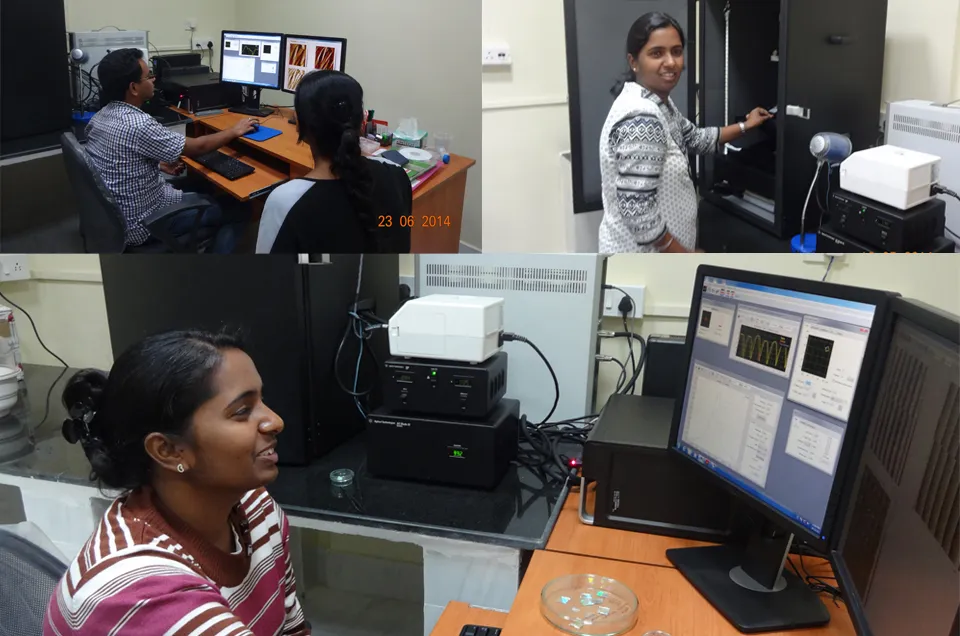
Scanning Probe Microscope (SPM)/ Atomic force microscope (AFM)
Specification of the Instrument:
Large scanner- 90µm × 90µm
Small scanner- 10µm × 10µm
Liquid cell Accessories
EFM
Closed Z loop for force measurement
Manufacturer details:
Agilent Technologies, Inc. (Now Taken over by Keysight)
| toll-free | +1 877-424-4536 |
| phone | +1 408-345-8886 |
| fax | +1 408 345-8474 |
| address | 5301 Stevens Creek Blvd
Santa Clara CA 95051, United States |
contact_us@agilent.com
Agilent Technologies India Pvt. Ltd.Registered Office
| phone | +91 11 46237100 |
| fax | +91 11 46237106 |
| address | Unit Nos. 105 - 116,
First Floor, Splendor Forum,
Plot No – 3, District Center Jasola,
New Delhi – 110025
India |
Purchase source (funding): Institute plan Grant
Year of installation: 2013
More information about the Instrument: http://www.home.agilent.com/en/pd-858475-pn-N9410S/atomic-force-microscope-afm-n9410s?&cc=IN&lc=eng
Sample Details
Instructions for Sample Preparation:
1. No loose powders, corrosive samples, liquids/vapours will be done .
2. One sample will roughly take 1 hour for imaging. Maximum three samples (same material) will be done in a 3 hours slot. Only two samples will be done if samples are of different materials .
3. Please DO NOT bring samples wrapped in tissue paper/ foil. Please bring samples in petry dish. Bring your own tweezers. Do not touch the sample with your hand .
4. Normally, imaging in intermittent contact mode (tapping mode) will be performed. You might have to wait longer for contact mode imaging.
5. Please do not bring very rough (roughness ~ 10 micron or higher) samples.
6. Maximum sample thickness is 5 mm.
7.Not all modes are available at any given time due to either set up constraints or other reasons.
8.For AFM max sample size is 15 mm x 15 mm and max sample thickness is < 5 mm. For MFM, sample must be limited to 6 mm x 6 mm, and for EFM sample must be LARGER than 10 mm x 10 mm.

Notable Results

Notable Results

Utility and Working Principle
The AFM consists of a cantilever with a sharp tip (probe) at its end that is used to scan the specimen surface. The cantilever is typically silicon or silicon nitride with a tip radius of curvature on the order of nanometers. When the tip is brought into proximity of a sample surface, forces between the tip and the sample lead to a deflection of the cantilever according to Hooke's law. Depending on the situation, forces that are measured in AFM include mechanical contact force, van der Waals forces, capillary forces, chemical bonding, electrostatic forces, magnetic forces (see magnetic force microscope, MFM), Casimir forces, solvation forces, etc. Along with force, additional quantities may simultaneously be measured through the use of specialized types of probes (see scanning thermal microscopy, scanning joule expansion microscopy, photothermal microspectroscopy, etc.).The AFM can be operated in a number of modes, depending on the application. In general, possible imaging modes are divided into static (also called contact) modes and a variety of dynamic (non-contact or "tapping") modes where the cantilever is vibrated or oscillated at a given frequency.