
Objective
X-ray Photoelectron Spectroscopy (XPS) also known as Electron Spectroscopy for Chemical Analysis (ESCA) is the most widely used surface analysis technique because it can be applied to a broad range of materials and provides valuable quantitative and chemical state information from the surface of the material being studied. The average depth of analysis for an XPS measurement is approximately 5 nm. The XPS instruments provide the ability to obtain spectra with a lateral spatial resolution as small as 7.5 µm. Spatial distribution information can be obtained by scanning the micro focused x-ray beam across the sample surface. Depth distribution information can be obtained by combining XPS measurements with ion milling (sputtering) to characterize thin film structures. The information XPS provides about surface layers or thin film structures is important for many industrial and research applications where surface or thin film composition plays a critical role in performance including: nanomaterials, photovoltaics, catalysis, corrosion, adhesion, electronic devices and packaging, magnetic media, display technology, surface treatments, and thin film coatings used for numerous applications.
Equipment & Details
X-ray Photoelectron Spectroscopy
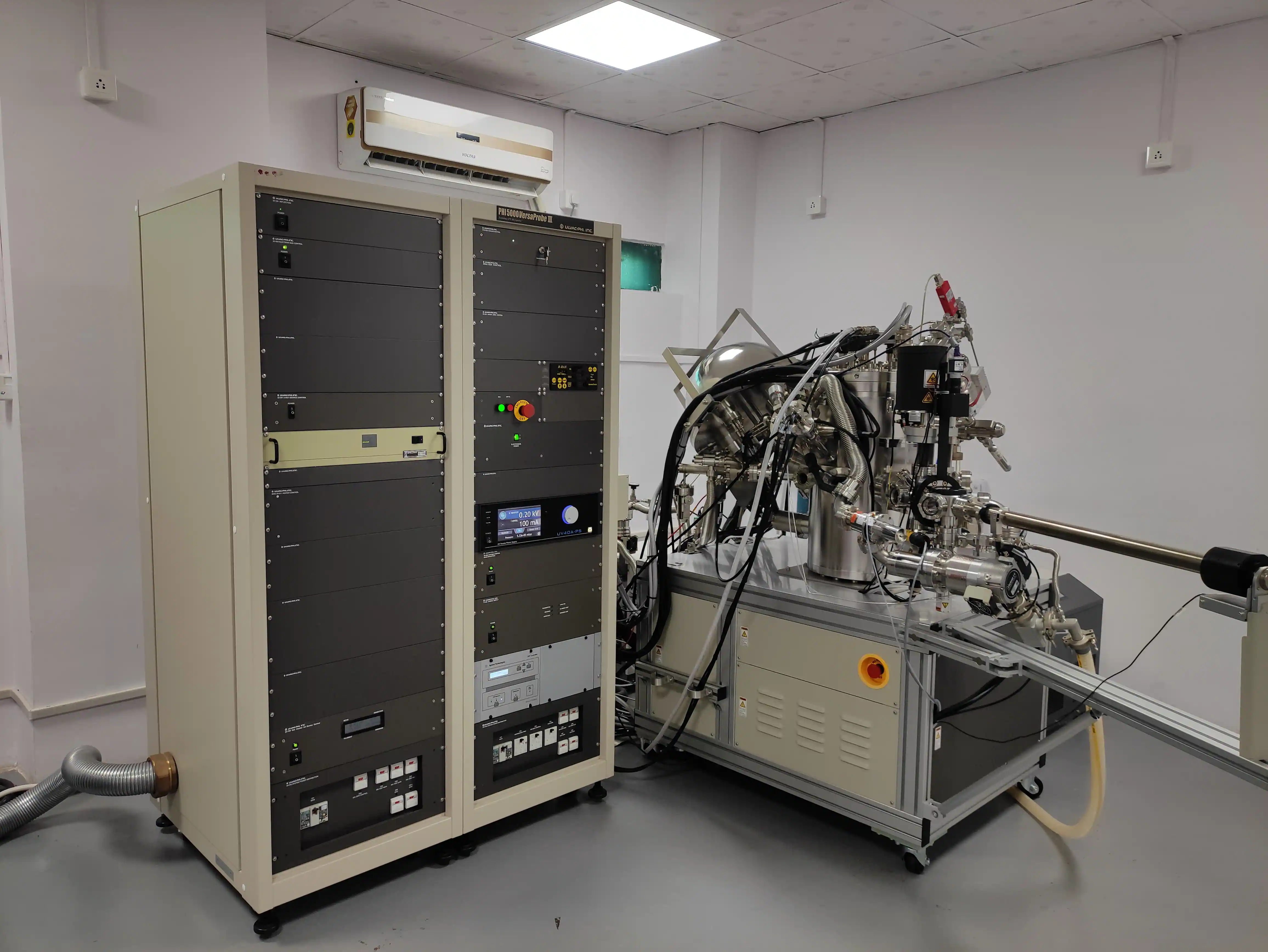
Model: PHI 5000 VERSA PROBE III
Manufacturer: ULVAC PHI(Physical Electronics), USA
XPS source: Monochromatic Al X-Ray Source with focused beam(< 10µm to 300 µm) for rapid X-ray induced Secondary electron Imagining (SXI)
Analyzer: A 180° hemispherical electron energy analyser supported with 128 channel detector
Argon Gun: 0- 5V argon ion gun for effective specimen cleaning depth profiling and charge neutralization
Sample heating & cooling: 800° C to -140° C
Gas Cluster Ion Source(GCIB): 2.5 to 20 kV Ar GCIB Gun for low damage surface cleaning
Ultraviolet Photoelectric Spectroscopy Source
Reflected Electron Energy Loss Spectroscopy (REELS)
Dual Anode: Magnesium and Zirconium twin anodes
Sample Details
The sample should be kept in oven overnight before submitting to the XPS Lab.
Thin film sample with low melting point(< 353 Kelvin) is not allowed
The powder sample should be converted to thin pellet (1-3 mm thickness). Loose Powder samples are not acceptable
The sample should not degas in Ultra high Vacuum
The sample should not contain radioactive, toxic and explosive materials
Sticky polymer films are not allowed. If polymers need to be analyzed, they need to be spin coated and dried
All kinds of spin-coated, drop-cast samples should be properly dried and desiccated.
Smaller sample dimensions are preferred. Sample with thickness ~1-2 mm and 5mm length/width/diameter are ideal.
Analysis on thin and thick films of all kinds of oil is not allowed.
Sample with Pb soldering is not allowed.
Note: The XPS lab reserve the right to reject any accepted analysis request at its discretion in the interest safety of the instrument and its operators.
Utility and Working Principle
X-ray photoelectron spectroscopy (XPS) is a surface characterization technique that can analyze a sample to a depth of 2 to 5 nanometres (nm). XPS is based on Einstein’s photoelectric effect in which x-ray beam containing k-alpha x-rays is focused on the sample. The absorption of incident x-rays results in the ejection of electrons. XPS is conducted in ultrahigh vacuum (UHV) conditions, around 10-9 millibar (mbar). In a typical XPS spectrum some of the photo-ejected electrons inelastically scatter through the sample enroute to the surface, while others undergo prompt emission and suffer no energy loss in escaping the surface and into the surrounding vacuum. Once these photo-ejected electrons are in the vacuum, they are collected by an electron analyzer that measures their kinetic energy. An electron energy analyzer produces an energy spectrum of intensity (number of photo-ejected electrons versus time) versus binding energy. Each prominent energy peak on the spectrum corresponds to a specific element.